
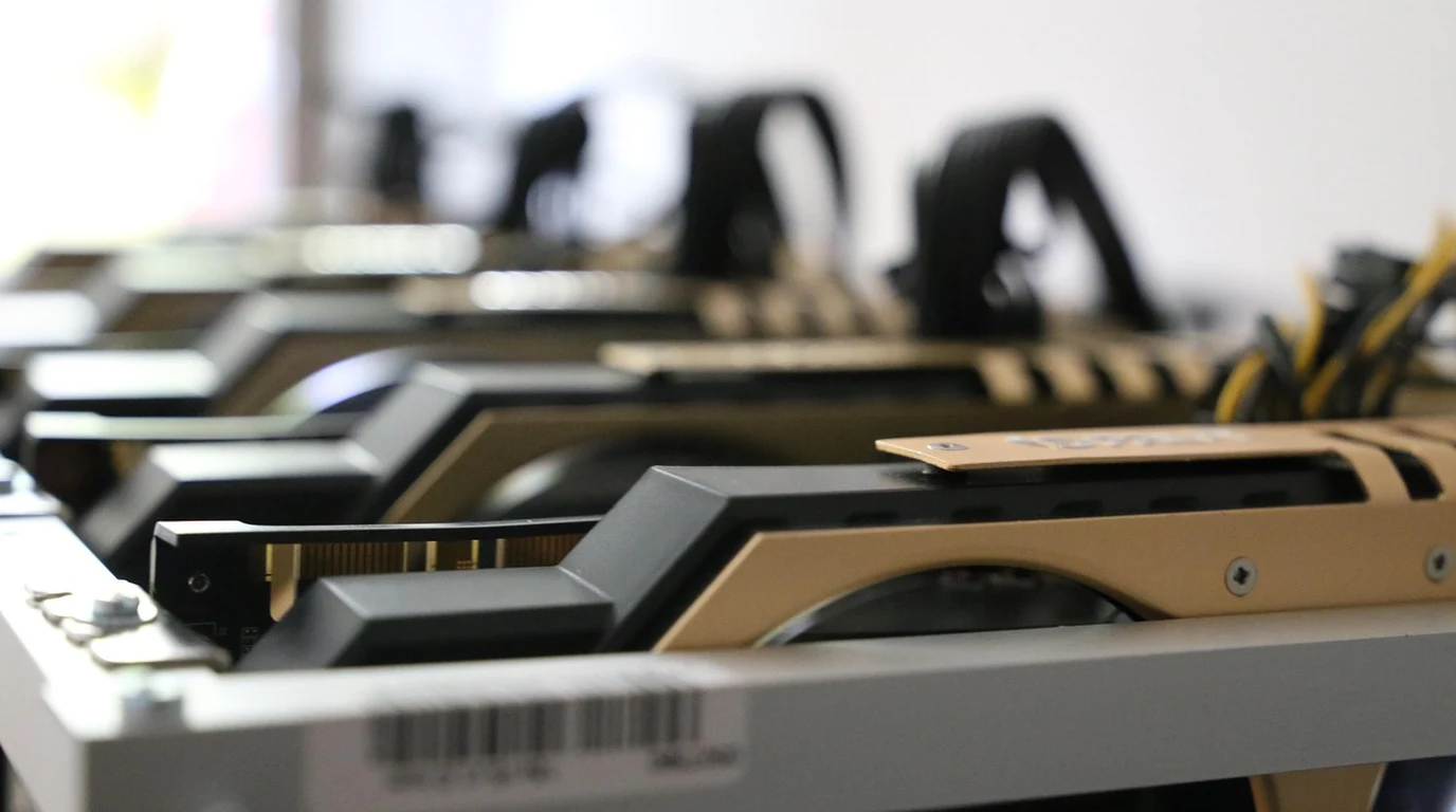
In the rapidly maturing domain of embedded edge artificial intelligence, edge engineers and robotics architects face a critical crossroads. Consumer single-board computers paired with low-cost USB or M.2 accelerators promise budget-friendly deployment, while full enterprise server racks provide unlimited FP16 compute at devastating power costs. Occupying the sweet spot of production-grade embedded edge compute is the NVIDIA Jetson Orin Nano Developer Kit and Production System-on-Module (SoM). Delivering up to 40 TOPS of dense INT8 tensor processing power in a form factor no larger than a standard credit card while consuming between 7W and 15W, the Orin Nano brings NVIDIA’s desktop Ampere GPU microarchitecture directly to autonomous robotics, industrial vision inspect, smart city infrastructure, and edge homelabs. Here is Kieran Mercer’s comprehensive forensic engineering masterclass on the NVIDIA Jetson Orin Nano: silicon architecture, TensorRT compilation workflows, INT8 calibration pipelines, unified memory bandwidth bottlenecks, power mode profiling, and total cost of ownership (TCO) ROI modeling.
What Makes the NVIDIA Jetson Orin Nano the Leading Edge AI Platform?
To understand the computational superiority of the Jetson platform, one must examine the fundamental architectural difference between an application-specific integrated circuit (ASIC) NPU and a general-purpose programmable GPU with dedicated tensor acceleration. Most edge NPUs are fixed-function systolic arrays. When a neural network architecture strictly matches their supported operator set (such as standard 2D convolutions or fixed-dimension matrix multiplications), they perform admirably. However, the moment a deep learning architecture introduces custom attention mechanisms, non-standard activation functions, dynamic sequence lengths, or complex post-processing logic, ASIC NPUs hit an operational wall, offloading unsupported operators to the weak host CPU and causing severe pipeline stalls.
The Jetson Orin Nano avoids this trap entirely by leveraging the full programmability of NVIDIA’s Ampere GPU Architecture. Equipped with 1,024 full-precision CUDA cores and 32 third-generation Tensor Cores, the GPU natively executes any arbitrary mathematical kernel written in CUDA, C++, or Triton. Third-generation Tensor Cores introduce hardware-accelerated Structural Sparsity (2:4 sparse matrix pattern acceleration), effectively doubling throughput on appropriately pruned deep learning weights without degrading operational accuracy.
Silicon Specifications & Microarchitectural Breakdown
Compare the microarchitecture, memory subsystem, and compute performance across the Jetson Orin product family:
| Hardware Specification | Jetson Orin Nano 4GB | Jetson Orin Nano 8GB | Jetson Orin NX 16GB |
|---|---|---|---|
| Peak INT8 Tensor Compute | 20 TOPS (Dense INT8) | 40 TOPS (Dense INT8) | 100 TOPS (Dense INT8) |
| GPU Microarchitecture | Ampere (512 CUDA / 16 Tensor) | Ampere (1,024 CUDA / 32 Tensor) | Ampere (1,024 CUDA / 32 Tensor) |
| CPU Architecture | 6-core Arm Cortex-A78AE v8.2 | 6-core Arm Cortex-A78AE v8.2 | 8-core Arm Cortex-A78AE v8.2 |
| Unified Memory Subsystem | 4GB 64-bit LPDDR5 (34 GB/s) | 8GB 128-bit LPDDR5 (68 GB/s) | 16GB 128-bit LPDDR5 (102 GB/s) |
| Configurable Power Modes | 5W / 7W / 10W | 7W / 15W | 10W / 15W / 20W / 25W |
| Hardware Video Encode (NVENC) | None (Software CPU / NVJPEG) | None (Software CPU / NVJPEG) | 1x 4K60 (H.264/H.265/AV1) |
| Production SoM Price (1k Unit) | ~$199 USD | ~$299 USD | ~$599 USD |
Unified Memory Architecture (UMA): Zero-Copy Ingestion
The most devastating performance penalty in multi-card edge systems—such as an x86 host connected to a PCIe accelerator—is the continuous memory copying across the PCIe bus. When a 4K camera frame is captured, it is initially buffered in host RAM. To perform AI inference on a discrete PCIe card, the host must execute a DMA transfer across the bus into the accelerator’s private device memory. Once inference completes, bounding box tensors must be copied back across the bus to host RAM for application consumption. This round-trip transfer introduces significant latency (5 to 15 ms) and consumes massive CPU cycles.
In contrast, the Jetson Orin Nano features a true Unified Memory Architecture (UMA). The 6-core Cortex-A78AE CPU and the 1,024-core Ampere GPU share a single, contiguous physical pool of 8GB high-speed LPDDR5 memory delivering 68 GB/s of bandwidth. By utilizing NVIDIA’s cudaHostAlloc() or Unified Virtual Memory (UVM) allocations, camera image buffers ingested via CSI-2 camera deserializers or Ethernet RTSP sockets reside directly in unified RAM. The GPU accesses the exact same physical memory address without a single memory copy, enabling sub-millisecond end-to-end pipeline latency from glass to inference.
Mastering TensorRT INT8 Quantization: Squeezing 40 TOPS
Deploying models in raw PyTorch or ONNX FP32 format leaves 75% to 80% of the Orin Nano’s computational power on the table. The 40 TOPS figure is achieved exclusively through INT8 Post-Training Quantization (PTQ) compiled with NVIDIA’s TensorRT inference engine. TensorRT optimizes the computational graph through horizontal and vertical layer fusion, kernel auto-tuning for Ampere Tensor Cores, and dynamic memory footprint minimization.
To convert an FP32 convolutional or transformer model to INT8 without losing bounding box detection accuracy, TensorRT uses an Entropy Calibrator (such as IInt8EntropyCalibrator2). During calibration, several hundred representative unlabelled validation images are passed through the network. TensorRT measures the dynamic range of activations at every layer, generating an optimal scaling factor that maps floating-point distributions into 8-bit signed integer values ($-128$ to $+127$). By minimizing Kullback-Leibler (KL) divergence, the calibrated INT8 engine achieves 99.2% of FP32 detection accuracy while slashing latency by 3.8x and cutting memory footprint in half.
Power Mode Profiling: Maximizing Watts-Per-Inference with nvpmodel
In autonomous drones, battery-powered rovers, and outdoor solar-powered edge enclosures, every watt of electrical dissipation dictates operational mission longevity. The Orin Nano incorporates NVIDIA’s dynamic power management daemon, controlled via the command-line utility nvpmodel.
Out of the box, the system supports two primary power modes:
- 15W MAXN Mode (nvpmodel -m 0): All 6 CPU cores operate at up to 1.5 GHz, the Ampere GPU clocks up to 625 MHz, and the LPDDR5 memory controller runs at maximum 2133 MHz. This mode unlocks the full 40 TOPS of INT8 inference throughput and maximizes multi-stream video decoding performance.
- 7W Low-Power Mode (nvpmodel -m 1): The CPU cluster is limited to 4 active cores clocked at 900 MHz, the GPU is capped at 400 MHz, and memory clock rates are dynamically throttled. In this mode, the system consumes less than 8 Watts at the wall under full continuous inference load, allowing completely fanless passive thermal enclosures in ambient environments up to 55°C.
The Total Cost of Ownership (TCO) ROI Model: Custom Silicon vs Jetson
When evaluating hardware selection for commercial edge AI products, engineering managers frequently commit the fatal mistake of comparing only unit hardware sticker prices. A $45 Chinese SBC paired with a $35 M.2 NPU accelerator appears on paper to save $200 per node compared to a $299 Jetson Orin Nano module. However, in production deployments, software engineering hours dominate the true Total Cost of Ownership (TCO).
Consider a commercial smart-city vision company deploying 500 edge nodes:
Custom NPU Toolchain Porting & Kernel Development (6 mo × 2 Sr Engineers @ $180k/yr): $180,000
Ongoing BSP Maintenance & Vulnerability Patching: $60,000/yr
Total Year 1 Cost for Budget Hardware: $290,000 ($580 per node)
Hardware Cost (500 units × $299 Jetson Orin Nano SoM): $149,500
Standard TensorRT Pipeline & JetPack Deployment (3 weeks × 1 Engineer): $10,500
NVIDIA Enterprise Long-Term Support (LTS) JetPack Updates: $0 (Included)
Total Year 1 Cost for Jetson Platform: $160,000 ($320 per node)
By leveraging NVIDIA’s polished JetPack SDK, pre-trained NGC model catalogs, DeepStream video streaming analytics frameworks, and ten-year production lifecycle commitments, the Jetson Orin Nano delivers an astonishing 44.8% reduction in total project expenditure while accelerating time-to-market by five months.
Kieran Mercer’s 6-Point Jetson Orin Nano Deployment Checklist
Before transitioning a Jetson Orin Nano from your homelab development bench into industrial field hardware, verify these six engineering requirements:
- Select High-Endurance NVMe Storage: The Orin Nano Developer Kit possesses no onboard eMMC or UFS flash; it boots exclusively from M.2 2280 Key-M NVMe storage. In industrial environments with continuous logging and frame caching, use high-endurance pSLC or industrial TLC NVMe drives rated for 1,000+ Terabytes Written (TBW).
- Account for Lack of Hardware NVENC: Remember that unlike the Orin NX, the Orin Nano silicon omits the dedicated hardware video encoder (NVENC). If your pipeline must record or re-stream outgoing H.264/H.265 video, utilize CPU GStreamer software encoding or integrate an external mini-PCIe hardware encoder chip.
- Implement Dynamic Thermal Throttling Monitoring: Monitor junction temperatures using
tegrastatsor the Jetson GPIO thermal trip pins. Ensure chassis thermal interface materials (TIM) maintain junction temperatures strictly below 85°C to avoid thermal clock degradation. - Pin Production Images to Long-Term Support (LTS) JetPack: Never deploy rolling developer previews in field units. Standardize your production images on validated JetPack 6.x LTS releases backed by Ubuntu 22.04 LTS and Linux Kernel 5.15.
- Enable Watchdog Timer (WDT) and Hardware Reset: Configure the internal Tegra hardware watchdog daemon (
/dev/watchdog) to automatically trigger a clean reboot if an application thread deadlocks or crashes in remote field installations. - Secure Boot and Disk Encryption: In commercial deployments where proprietary model weights reside on external NVMe drives, enable NVIDIA’s Fuse-based Secure Boot and LUKS-encrypted root filesystem to protect intellectual property from physical hardware extraction.
End-to-End Vision Pipelines: NVIDIA DeepStream & GStreamer Zero-Copy
In production computer vision, raw model inference throughput is only one piece of the performance equation. A vision system must decode incoming video streams, convert pixel formats from YUV to RGB, scale images, normalize tensors, execute inference, track objects across temporal frames, and render bounding box overlays. If each of these stages performs an independent memory copy into CPU space, the Cortex-A78AE CPU cores become 100% saturated with memory management tasks, choking the GPU.
To eliminate this bottleneck, NVIDIA provides the DeepStream SDK, built directly on top of the open-source GStreamer multimedia framework. DeepStream utilizes hardware-accelerated GStreamer plugins—such as nvv4l2decoder for hardware video decoding, nvvideoconvert for hardware-accelerated color space conversion, and nvinfer for direct TensorRT inference dispatch. By passing standardized NvBufSurface hardware memory pointers between pipeline elements, video frames travel from the network socket through decode, scaling, inference, and Kalman-filter object tracking (via NvDCF or DeepSORT) entirely within contiguous GPU memory without a single CPU host memory copy. This architectural pipeline enables a single 15W Jetson Orin Nano to seamlessly process eight concurrent 1080p 30 FPS H.265 RTSP security camera feeds executing real-time object detection and trajectory tracking with sub-30 millisecond glass-to-display latency.
While Jetson represents the high-end proprietary edge standard, open-source silicon is advancing rapidly. Connect your hardware analysis with our study on Milk-V Mars vs StarFive VisionFive 2: RISC-V SBC Lab.