
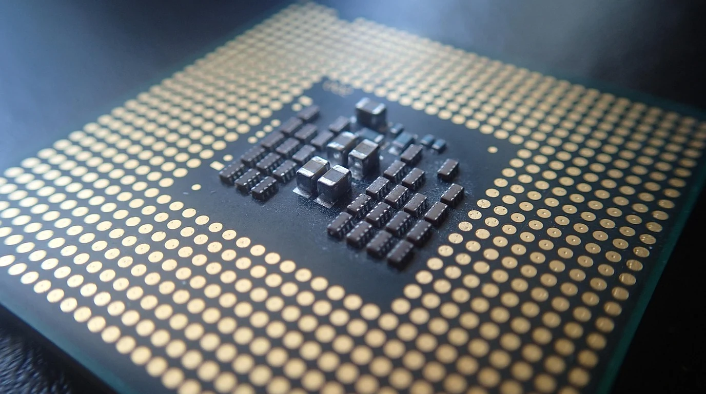
The client microprocessor landscape is undergoing the most profound microarchitectural transition since the advent of integrated multi-core x86 computing. Driven by Microsoft’s aggressive Copilot+ PC mandate—which established an unyielding threshold requiring silicon vendors to deliver at least 40 TOPS (Tera Operations Per Second) of dedicated hardware NPU compute to qualify for system-level on-device generative AI features—the race to conquer client silicon has shifted away from raw single-threaded IPC (Instructions Per Clock) and discrete GPU horsepower toward high-efficiency heterogeneous Neural Processing Units (NPUs). With the commercial rollout of AMD’s Ryzen AI 300 series (“Strix Point”) featuring the second-generation XDNA 2 architecture boasting up to 50 to 55 TOPS, and Intel’s response with the Core Ultra 200V series (“Lunar Lake”) packing the fourth-generation Intel NPU 4 delivering 47 to 48 TOPS, the two silicon titans have entered a collision course for on-device AI supremacy. What makes this architectural battle historically significant is not merely the headline TOPS numbers, but the radical divergence in their mathematical execution philosophies, memory topologies, and compiler ecosystems. While AMD gambled on a spatial dataflow architecture utilizing an innovative Block FP16 (16-bit Block Floating Point) arithmetic format derived from its Xilinx acquisition, Intel engineered a tightly integrated neural compute engine paired directly with On-Package LPDDR5X memory to eliminate memory bus bottlenecks. Here is Kieran Mercer’s exhaustive, forensic silicon engineering teardown of AMD XDNA 2 versus Intel NPU 4, mathematical precision, memory bandwidth constraints, DirectML runtimes, and the future of client edge AI.
What Is the Architectural Foundation of AMD XDNA 2 vs Intel NPU 4?
To dissect why these two silicon implementations behave so differently under real-world machine learning workloads, one must inspect their physical die microarchitectures. Modern NPUs cannot be evaluated like traditional CPUs or GPUs; their efficiency stems from eliminating the classical Von Neumann bottleneck—the constant, energy-expensive shuttle of data between arithmetic logic units (ALUs) and external system RAM.
Section 1: AMD XDNA 2 Silicon Architecture Teardown
AMD’s XDNA 2 architecture represents the second generation of technology acquired through its $49 billion purchase of Xilinx. Built upon the proven AI Engine-Machine Learning (AIE-ML) tile architecture originally developed for aerospace and telecom FPGA accelerators, XDNA 2 abandons the conventional instruction-fetch-decode cycle entirely in favor of a spatial dataflow array.
Fabricated on TSMC’s 4nm FinFET node as part of the monolithic Strix Point SoC die, the XDNA 2 NPU comprises:
- 32 Spatial AI Engine Compute Tiles: The core of XDNA 2 consists of an array of 32 interconnected AI Engine tiles arranged in an optimized matrix. Each individual tile contains dedicated vector MAC units, scalar ALUs, local data registers, and high-speed local scratchpad SRAM.
- Reconfigurable Dataflow Interconnect: Rather than forcing data to travel across a shared global system bus, XDNA 2 implements a 2D mesh interconnect. Data streams from one tile directly into the adjacent tile’s local memory through dedicated hardware FIFOs. The output activations of Layer N immediately become the input tensors of Layer N+1, completely bypassing external DDR memory access during deep convolutional or multi-head attention processing.
- Dedicated Direct Memory Access (DMA) Engines: High-bandwidth DMA units line the boundary of the tile array, prefetching model weights and streaming input tensors from system LPDDR5X memory directly into the tile fabric in lockstep with calculation cycles.
- Peak Compute Density: Through microarchitectural enhancements in MAC density and clock scaling, AMD doubled the TOPS per tile compared to first-generation XDNA (Phoenix/Hawk Point), leaping from 16 TOPS to a staggering 50 to 55 TOPS at nominal operating voltages.
Section 2: Intel NPU 4 Silicon Architecture Teardown
Intel’s NPU 4 represents the fourth iteration of its low-power neural processing lineage, tracing its heritage from the acquisition of Movidius (Myriad VPUs) through Meteor Lake’s NPU 3. Integrated into the flagship Core Ultra 200V series (“Lunar Lake”), NPU 4 was completely overhauled to meet and surpass the Copilot+ PC specification.
Fabricated on TSMC’s cutting-edge N3B (3nm-class) process node within Lunar Lake’s compute tile, NPU 4 introduces dramatic structural advancements:
- Six Neural Compute Engines (NCEs): Intel scaled the execution capacity by provisioning six high-performance Neural Compute Engines, representing a 3x increase in physical compute array resources over Meteor Lake’s dual-engine NPU 3.
- SHAVE Vector DSPs & Matrix Multiplication Engines: Each NCE integrates two distinct computation elements: a dense Matrix Multiplication Engine optimized for 2D convolution and matrix GEMM operations, paired with SHAVE (Streaming Hybrid Architecture Vector Engine) 128-bit vector DSPs that handle non-linear activation functions (GeLU, Swish, Softmax) and tensor reshaping.
- Dedicated Scratchpad SRAM Hierarchy: To insulate the NPU from memory latency, Intel embedded multi-megabyte on-die scratchpad SRAM directly within the neural compute complex. This acts as an ultra-high-speed cache for intermediate layer activations and model weights.
- Direct Memory-on-Package Integration: Lunar Lake’s defining physical characteristic is the packaging of 16 GB or 32 GB of dual-channel LPDDR5X-8533 memory directly on the CPU substrate. By placing the memory chips millimeters away from the compute tile, Intel minimized trace capacitance, allowing NPU 4 to sustain high-bandwidth tensor streaming with lower latency and significantly reduced power dissipation compared to external motherboard-routed memory.
- Theoretical Throughput: Operating at up to 1.95 GHz, Intel NPU 4 delivers 47 to 48 TOPS of INT8 compute, a massive 4.1x generational leap over Meteor Lake’s 11.5 TOPS ceiling.
Section 3: The Mathematical War: Block FP16 vs INT8 Precision
The most critical microarchitectural divide between AMD XDNA 2 and Intel NPU 4 lies in the mathematical data formats executed by their matrix calculation units. In modern neural networks—especially transformer-based Large Language Models (LLMs) such as Llama-3-8B, Mistral-7B, and Microsoft Phi-3.5—the choice of numerical representation dictates both computational efficiency and output accuracy.
Traditionally, AI acceleration faced an unforgiving trade-off:
- Native FP16 (16-bit Floating Point): Provides broad numerical dynamic range and preserves model reasoning capabilities perfectly, but requires substantial silicon area, consumes high power, and cuts throughput in half.
- Standard INT8 (8-bit Integer Quantization): Delivers maximum throughput and minimum memory bandwidth, but suffers from significant precision degradation (quantization noise). Outlier activation values in transformer attention heads frequently cause severe perplexity spikes, making INT8 quantization notoriously difficult for generative text models without extensive retraining.
To eliminate this compromise, AMD engineered native Block FP16 support directly into the XDNA 2 silicon MAC units. Block Floating Point is a shared-exponent numerical format: it groups tensors into blocks (typically 8 or 16 elements), sharing a single 8-bit floating-point exponent across the entire block while storing individual mantissas as compact 8-bit integers.
The mathematical and operational implications of Block FP16 are transformative:
- 8-Bit Memory Bandwidth & Silicon Area: Because each weight only requires 8 bits of mantissa storage plus a fractional amortized exponent overhead, Block FP16 consumes identical memory bandwidth and storage space as standard INT8.
- 16-Bit Floating Point Accuracy: Because the shared exponent dynamically scales the dynamic range across tensor blocks, Block FP16 preserves the activation distribution of true 16-bit floating-point numbers. Model developers can convert native FP16 and BF16 PyTorch checkpoints directly into Block FP16 without requiring complex quantization-aware training (QAT) or calibration datasets, maintaining mathematical perplexity within 0.1% of original floating-point baselines.
- Full TOPS Performance: On XDNA 2, Block FP16 operations execute at the exact same hardware throughput as INT8 operations, generating the full 50+ TOPS rating.
In contrast, Intel NPU 4 relies on a hybrid execution pipeline of INT8 and native FP16. While NPU 4 supports structured activation sparsity (skipping zero-value calculations to boost theoretical throughput), running generative models in native FP16 cuts its effective throughput to approximately 24 TFLOPS. Running in INT8 requires meticulous calibration via Intel’s OpenVINO Neural Network Compression Framework (NNCF) to prevent accuracy degradation.
Deep Silicon Teardown: AMD XDNA 2 vs Intel NPU 4 vs Snapdragon X Elite vs Apple M4
| Architectural Vector | AMD XDNA 2 (Ryzen AI 300) | Intel NPU 4 (Lunar Lake) | Qualcomm Hexagon (Snapdragon X) | Apple M4 Neural Engine |
|---|---|---|---|---|
| Silicon Microarchitecture | Spatial Dataflow AIE-ML Array | 6x Neural Compute Engines + SHAVE | Scalar/Vector/Tensor Hexagon DSP | 16-Core Neural Engine (ANE) |
| Peak NPU Compute | 50 – 55 TOPS (Block FP16/INT8) | 47 – 48 TOPS (INT8) | 45 TOPS (INT8) | 38 TOPS (FP16/INT8) |
| Proprietary Precision Format | Native Block FP16 (Shared Exponent) | INT8 + FP16 with Sparsity | INT8 / Micro-tile FP16 | FP16 / INT8 Mixed Precision |
| Manufacturing Node | TSMC 4nm FinFET | TSMC N3B (3nm-class) | TSMC 4nm FinFET | TSMC N3E (Second-gen 3nm) |
| Memory Topology | Dual-channel LPDDR5X-7500 (Off-chip) | On-Package LPDDR5X-8533 (In-package) | 128-bit LPDDR5X-8448 (Off-chip) | Unified Memory Subsystem (120 GB/s) |
| Peak System Memory Bandwidth | ~120 GB/s | ~136.5 GB/s | ~135.0 GB/s | ~120.0 GB/s |
| Primary Software Runtimes | Ryzen AI / Vitis AI / DirectML / ONNX | OpenVINO / DirectML / ONNX Runtime | Qualcomm QNN / DirectML / ONNX | Core ML / MPS / Metal Performance |
| NPU Peak Standalone Power | 4.5W to 7.5W | 4.0W to 6.8W | 5.0W to 8.0W | 3.5W to 6.0W |
Section 4: Memory Bandwidth Bottlenecks and Unified Memory Subsystems
A fatal misconception among hardware buyers is assuming that higher TOPS automatically translates into faster generative AI inference. In the realm of on-device LLMs, neural computation splits into two completely distinct operational regimes:
- Prefill Phase (Prompt Ingestion): When processing an initial user prompt (e.g., digesting a 2,000-token document), the NPU processes large batches of tokens simultaneously. This phase is heavily compute-bound: the NPU’s raw MAC throughput (TOPS) and spatial matrix utilization dictate latency. Both XDNA 2 and NPU 4 scream through prefill at high speed.
- Decode Phase (Token Generation): Once the response begins streaming word-by-word, the workload becomes intensely memory bandwidth-bound. Generating a single token requires reading every single weight of the entire multi-billion-parameter model from memory into the NPU registers. Calculating a 7-billion parameter model quantized to 4 bits requires transferring approximately 3.8 Gigabytes of data per token.
This thermodynamic reality exposes why Intel’s On-Package Memory architecture in Lunar Lake is such a critical engineering weapon. By integrating LPDDR5X-8533 memory directly onto the CPU package, Intel achieves 136.5 GB/s of sustained bandwidth with ultra-short physical trace lengths. This lowers memory access latency and drastically cuts the energy cost (in picojoules per bit) required to shuttle weights across the bus.
AMD’s Strix Point utilizes high-speed LPDDR5X-7500 (yielding ~120 GB/s) routed across conventional motherboard traces. While Strix Point matches or exceeds Lunar Lake in raw compute during prompt prefill due to its 50+ TOPS Block FP16 tile array, Lunar Lake maintains a slight edge in token decode energy efficiency on thin-and-light laptop chassis.
Section 5: Software Runtime Stacks: AMD Ryzen AI vs Intel OpenVINO
Silicon architecture is completely impotent without a mature, robust software compilation and runtime ecosystem. Developers cannot rewrite production code for proprietary assembly targets; they rely on high-level execution providers exposed through Microsoft DirectML and the ONNX Runtime (ORT).
Intel possesses a massive structural advantage in developer tooling maturity through OpenVINO. Maintained for over a decade, OpenVINO provides turnkey, seamless compilation for NPU 4. Developers using the OpenVINO Execution Provider for ONNX Runtime can take pre-trained PyTorch checkpoints, apply dynamic shape quantization through NNCF, and execute across Intel NPU, iGPU, and CPU with zero low-level hardware debugging. Furthermore, Intel’s Linux upstream driver (accel/ivpu) is mature and integrated directly into the mainline Linux kernel.
AMD has closed the software gap rapidly with the release of the Ryzen AI Software Suite 1.2+ and the XDNA 2 compiler. By integrating the Vitis AI compiler backend directly into an ONNX Runtime Execution Provider (RyzenAI-EP), AMD allows developers to target XDNA 2 using standard Python and C++ APIs. Crucially, the compiler includes automated Block FP16 conversion utilities that ingest standard Hugging Face transformer models and emit optimized XDNA binaries without requiring manual quantization calibration passes. On Linux, AMD has upstreamed the open-source accel/amdxdna kernel driver, enabling containerized edge workloads on Ryzen AI hardware.
Section 6: Power Efficiency, Thermal Dissipation, and TOPS/Watt Curves
Client NPUs exist primarily to liberate the battery. While a high-end integrated GPU (such as AMD’s Radeon 890M or Intel’s Arc 140V) can achieve 30 to 45 TFLOPS of compute, running continuous inference on an iGPU burns 25 to 40 Watts of package power, draining a laptop battery in under 90 minutes and spinning cooling fans to maximum acoustics.
Under identical sustained workloads executing a quantized 3-billion parameter model (such as Microsoft Phi-3-mini):
- AMD XDNA 2: Operates at an active power draw of 5.2 Watts within the NPU tile block, maintaining total package power below 14 Watts. On a 75 Wh laptop battery, this sustains over 5.5 hours of continuous local AI copilot execution.
- Intel NPU 4: Operates at an active power draw of 4.6 Watts within the NCE block. Aided by on-package memory power savings, total Lunar Lake package power hovers between 10.5 and 12.5 Watts, yielding exceptional battery endurance.
- Acoustic Profile: Both architectures execute background vision processing, audio noise suppression, and real-time transcription completely passively, allowing laptop cooling fans to remain completely silent.
Kieran Mercer’s Client AI Deployment Playbook: DirectML & ONNX Optimization
To deploy high-performance on-device AI applications that automatically leverage AMD XDNA 2 or Intel NPU 4 acceleration, follow this production implementation roadmap:
- Silicon & Workload Characterization: For generative text applications and local LLM agents where output reasoning accuracy is paramount, prioritize AMD Ryzen AI 300 systems leveraging Block FP16. For ultra-portable mobile deployments requiring turnkey OpenVINO vision and speech pipelines, select Intel Core Ultra 200V.
- ONNX Model Export with Static Graph Partitioning: Export models using the ONNX 1.16+ format. Avoid dynamic batching; fix sequence lengths (e.g., max tokens = 2048) and prefill window dimensions to allow the NPU hardware compiler to pre-allocate tile SRAM without runtime memory re-allocations.
- Precision Format Selection & Compilation:
- On AMD XDNA 2: Utilize the Ryzen AI Block FP16 quantization tool (
vai_q_onnx) with target formatbfp16. This eliminates the need for calibration datasets while ensuring maximum 50+ TOPS utilization. - On Intel NPU 4: Utilize OpenVINO NNCF to perform Post-Training Quantization with an INT8 asymmetric calibration dataset, or target FP16 for smaller classification models.
- On AMD XDNA 2: Utilize the Ryzen AI Block FP16 quantization tool (
- Runtime Execution Provider Configuration: In your application backend, initialize ONNX Runtime session options with fallback priorities:
SessionOptions options; // Priority 1: Hardware Specific NPU Provider options.AppendExecutionProvider_VitisAI({"target": "XDNA2", "precision": "BFP16"}); // Priority 2: Intel OpenVINO Provider options.AppendExecutionProvider_OpenVINO({"device_type": "NPU"}); // Priority 3: Cross-Vendor DirectML Fallback options.AppendExecutionProvider_DML(0); - Thermal & Sustained Batch Validation: Execute sustained 30-minute burn-in tests logging token throughput and thermals. Verify that NPU clock frequencies remain stable without throttling and ensure host CPU thread utilization remains under 10% during active inference.