
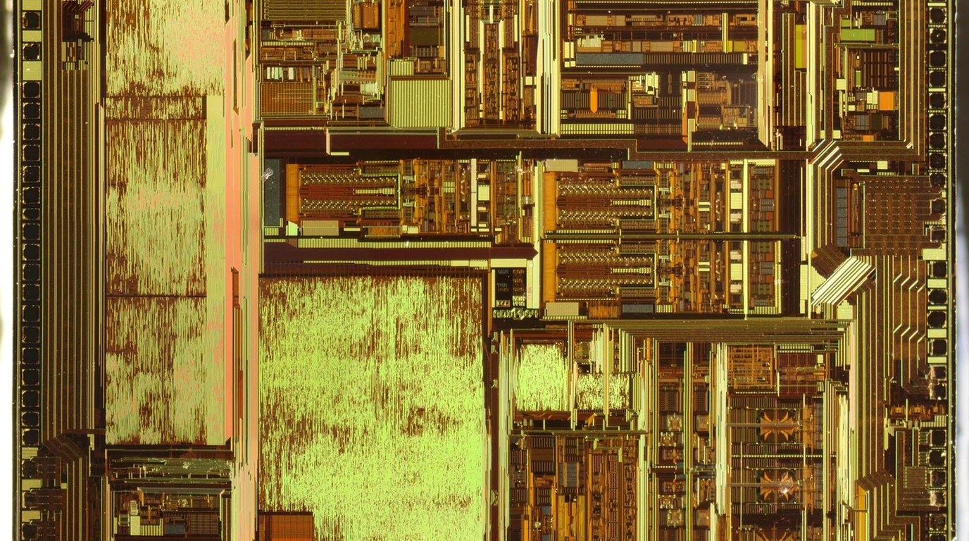
While mainstream enterprise datacenters remain locked in an expensive, supply-constrained duopoly between Nvidia CUDA GPUs and hyperscale custom ASICs (Google TPU, AWS Trainium), an architectural revolution is quietly detonating at the edge. Next-generation semiconductor startups are discarding legacy von Neumann compute grids in favor of radical new silicon paradigms: Digital In-Memory Computing (D-IMC) and open-source RISC-V Tensix spatial compute arrays. Spearheading this frontier are Europe’s Axelera AI with its Metis AIPU and Jim Keller’s Tenstorrent with its Wormhole and Blackhole RISC-V processors. How do their microarchitectures, native numeric formats, and compiler philosophies compare?
What Is the Difference Between Axelera Metis and Tenstorrent Wormhole?
Axelera Metis AIPU delivers 214 TOPS at 35W utilizing Digital In-Memory Computing (D-IMC) where matrix multiplications are performed directly inside custom SRAM cells, optimized for high-throughput edge computer vision. Tenstorrent Wormhole delivers an open-architecture spatial grid of 72 Tensix cores powered by custom 64-bit RISC-V processors, running native FP8/BF16 matrix mathematics via open-source compilers (TT-Metalium/TT-Buda) to accelerate both vision and generative LLMs.
To appreciate why these architectures represent the future of post-GPU silicon, one must examine the “Memory Wall”. In conventional GPUs and CPUs, over 70% of total electrical energy and execution latency is expended simply moving weight matrices and activation tensors back and forth across high-speed memory buses between DRAM chips and register files. Compute is cheap; memory transport is extraordinarily expensive.
Axelera Metis AIPU obliterates the memory wall through Digital In-Memory Computing. Developed in the Netherlands, Axelera’s silicon integrates four heterogeneous compute tiles containing proprietary D-IMC SRAM blocks. In standard computing, data is fetched from SRAM, brought to an ALU, multiplied, and written back. In Axelera’s D-IMC silicon, the multiply-accumulate operation takes place directly inside the digital SRAM bit-cell matrix itself. By eliminating the physical movement of weights, the Metis AIPU achieves an astonishing compute density of 214 TOPS (INT8) on an M.2 or PCIe card drawing just 35 watts, sustaining over 3,200 FPS on ResNet-50.
Tenstorrent, led by legendary microprocessor architect Jim Keller (lead architect of AMD Zen, Apple A4/A5, and Tesla Autopilot silicon), takes an entirely different philosophical path: programmable RISC-V spatial arrays. Rather than fixed-function in-memory blocks, the Tenstorrent Wormhole architecture features an array of Tensix cores arranged in a 2D mesh interconnected by a high-bandwidth Network-on-Chip (NoC). Each Tensix core contains five small, highly efficient 64-bit RISC-V microprocessors operating in tandem with specialized matrix and vector processing units. Wormhole does not treat neural networks as static compiled circuits; it treats them as dynamic, routed data packets flowing across a programmable grid of open-source RISC-V cores.
Axelera Metis vs Tenstorrent Wormhole: Silicon Comparison Matrix
Comparing microarchitectural philosophies, native numerical formats, compiler openness, and target workloads:
| Silicon Metric | Axelera Metis AIPU (PCIe / M.2) | Tenstorrent Wormhole n150 (PCIe Gen4) | Architectural Advantage |
|---|---|---|---|
| Execution Core Philosophy | Digital In-Memory Computing (D-IMC) | 72x Spatial RISC-V Tensix Cores | Tenstorrent provides fully programmable RISC-V flexibility. |
| Peak Compute Horsepower | 214 TOPS (INT8 Precision) | 262 TFLOPS (FP8) / 131 TFLOPS (BF16) | Tenstorrent natively accelerates floating-point LLM math. |
| On-Chip Memory & Bandwidth | Embedded D-IMC SRAM (>50 TB/s internal) | 12GB GDDR6 (288 GB/s Bandwidth) | GDDR6 accommodates 8B to 14B parameter language models. |
| Software Compiler Stack | Voyager SDK (ONNX / PyTorch export) | TT-Metalium & TT-Buda (100% Open Source) | Tenstorrent eliminates proprietary software black boxes. |
| Board Thermal Envelope (TDP) | 15W (M.2 module) to 35W (PCIe card) | 160W (PCIe Gen4 Standard Slot) | Axelera operates in fanless industrial edge enclosures. |
Open Source Silicon Software: The Anti-CUDA Movement
The defining distinction of Tenstorrent is its radical commitment to open-source compiler infrastructure. Nvidia’s dominance is underpinned by CUDA—a closed, proprietary software stack that locks developers to Nvidia silicon. Tenstorrent open-sourced its entire low-level programming layer, TT-Metalium, allowing developers to program the RISC-V Tensix cores directly in bare-metal C++ with zero licensing tolls.
Above TT-Metalium sits TT-Buda, an automated graph compiler that ingests models directly from PyTorch, JAX, and ONNX. If a developer invents a brand-new attention mechanism or non-standard transformer layer tomorrow, they do not have to wait six months for a semiconductor vendor to release a closed driver update. Developers can write their own custom RISC-V microcode to run the new operator natively across the core mesh.
Analog vs Digital In-Memory Computing: The Noise-Immunity Moat of D-IMC
To evaluate Axelera AI’s breakthrough, one must differentiate between two competing branches of in-memory processing: Analog In-Memory Computing (A-IMC) and Digital In-Memory Computing (D-IMC).
Historically, startups attempted to build in-memory computing using analog circuits: representing numbers as electrical current or voltage levels and performing matrix multiplication via Ohm’s and Kirchhoff’s laws inside memristors, phase-change memory (PCM), or flash cells. While analog IMC promises theoretical ultra-high efficiency, it is notoriously plagued by physical thermal drift, manufacturing process variations, and analog-to-digital converter (ADC) noise, which degrades neural inference accuracy and causes models to drift over time.
Axelera Metis completely eliminates this vulnerability by engineering 100% Digital In-Memory Computing (D-IMC). Axelera’s bit-cells perform mathematical operations using pure digital logic gates embedded within the SRAM cell layout. There are no noisy ADCs, no analog current variations, and no temperature-induced accuracy drift. Axelera achieves mathematical bit-exact deterministic results that match standard x86 and GPU calculations, while slashing memory transport energy by up to 70%.
Tenstorrent Multi-Chip Scaling: 100GbE Optical Mesh Networks
While Axelera targets ultra-efficient single-card edge vision appliances, Tenstorrent’s Wormhole architecture is engineered for limitless modular scaling. At the physical die edge, each Wormhole processor integrates six 100-Gigabit Ethernet (100GbE) optical interfaces directly into the silicon package.
This allows systems engineers to connect multiple Tenstorrent cards directly together using low-latency optical QSFP-DD cables, creating a seamless 2D torus or all-to-all mesh topology without requiring expensive external enterprise Ethernet switches or proprietary Nvidia NVLink switch boards. Tensors flow across chip boundaries directly through the on-chip Network-on-Chip (NoC), allowing an array of four to sixteen Wormhole processors to operate as a single, unified multi-teraflop computing cluster capable of running 70-billion parameter generative AI models at the enterprise edge.
Enterprise Workload Mapping: Computer Vision vs Generative LLMs
When selecting between these emerging silicon platforms for commercial infrastructure deployments, target workload mapping dictates the winner:
- Deploy Axelera Metis For: High-density, multi-camera computer vision in branch offices, logistics hubs, and industrial robotics. If you need to run YOLOv8, OCR text extraction, and segmentation across 32 concurrent 4K video feeds in an unventilated 35W industrial DIN-rail enclosure, Axelera Metis delivers unbeatable efficiency.
- Deploy Tenstorrent Wormhole For: Localized Generative AI, Retrieval-Augmented Generation (RAG), and open-source foundation model experimentation. Wormhole’s 12GB of GDDR6 memory and native BF16/FP8 precision allow hosting Llama-3-8B and Mistral-7B locally, scaling seamlessly into multi-card mesh clusters via onboard 100GbE optical ethernet interconnects without PCIe switch bottlenecks.
Frequently Asked Questions About Emerging Edge AI Silicon
What is Digital In-Memory Computing (D-IMC)?
D-IMC performs mathematical multiply-accumulate operations directly inside digital SRAM storage cells, eliminating the energy-intensive transfer of neural weights across external memory buses.
Can Tenstorrent Wormhole run PyTorch models directly?
Yes. Tenstorrent’s open-source TT-Buda and TT-Forge toolchains compile standard PyTorch models directly to run across the RISC-V Tensix core grid.
Are Axelera Metis accelerators available in standard M.2 slots?
Yes. Axelera manufactures the Metis AIPU in a standard M.2 Key M 2280 module operating at 15 watts, as well as a full PCIe Gen4 add-in card operating at 35 watts.
Ultra-Low Power Transformer Accelerators
Post-GPU silicon targets ultra-dense spatial transformer acceleration at edge power budgets. Review sub-5W dedicated neural processors in our breakdown on Kneron KL730 vs Hailo-8: Sub-5W Edge AI Guide.
Spatial dataflow architectures challenge monolithic GPU paradigms. Review next-gen neuromorphic and RISC-V silicon in our masterclass on Tenstorrent Wormhole: RISC-V Tensix Architecture Guide.