
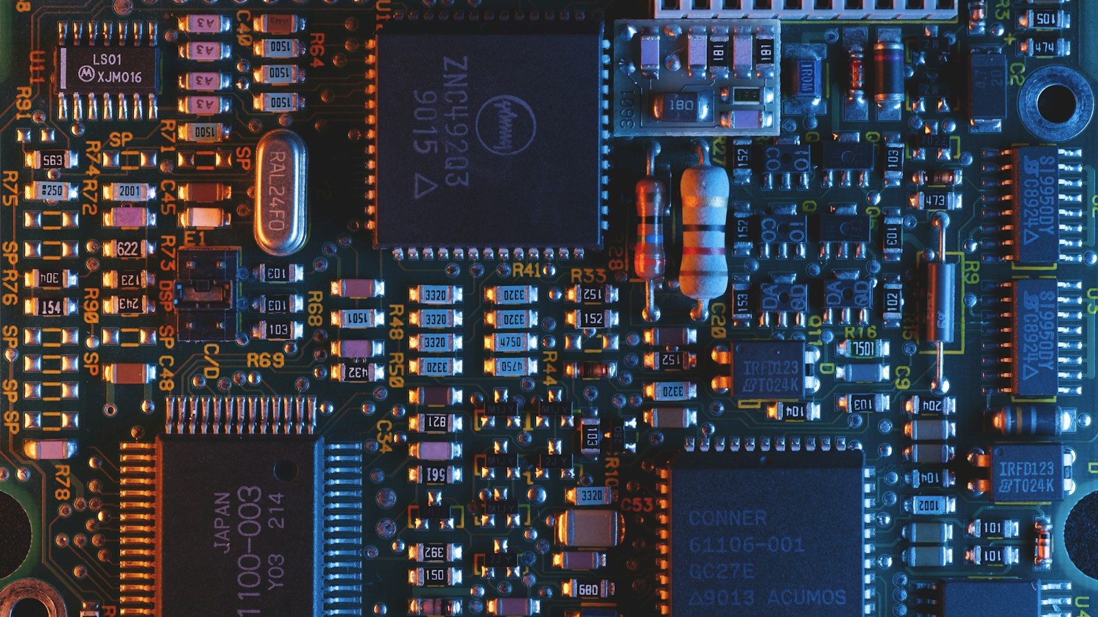
The proliferation of computer vision, edge robotics, autonomous drones, and smart estate surveillance in 2026 has pushed edge silicon to a critical inflection point. Systems architects can no longer rely on general-purpose ARM CPUs or power-hungry desktop GPUs for low-latency inferencing at the edge. The industry has decisively shifted toward specialized silicon: dedicated Neural Processing Units (NPUs), systolic tensor arrays, and low-power embedded GPU system-on-chips (SoCs).
Yet navigating the procurement and hardware integration landscape is fraught with engineering trade-offs. Datasheets routinely flaunt theoretical peak INT8 TOPS computed as simple arithmetic products (Frequency × MAC Units × 2), completely obscuring memory bus saturation, thermal throttling curves, operator fallback penalties, and the compiler friction that determines whether a deployed model runs in hardware or grinds host CPU cores to 100% saturation.
At Edge Silicon Lab, our mandate is rigorous, bare-metal silicon forensics. In this benchmark teardown, we pit the three dominant edge accelerators against each other under identical laboratory conditions: the venerable Google Coral Edge TPU (28nm ASIC), the high-efficiency Hailo-8 M.2 (16nm TSMC dataflow processor), and the unified powerhouse NVIDIA Jetson Orin Nano 8GB (8nm Samsung Ampere SoC). We dissect their microarchitectures, analyze roofline models, evaluate batch-1 latencies across modern vision backbones, and expose the real-world interconnect traps that silently degrade edge pipeline throughput.
1. The TOPS/Watt Fallacy: Peak Theoretical Arithmetic vs. Sustained Tensor Throughput
To understand why edge accelerators perform so disparately, we must examine the physical physics of deep neural network inferencing. Deep learning inferencing consists primarily of dense matrix multiplications (GEMM) and multi-dimensional convolutions. An INT8 Multiply-Accumulate (MAC) operation takes two 8-bit integers, multiplies them into a 16-bit intermediate product, and accumulates the result into a 32-bit register.
Manufacturers compute theoretical peak TOPS using the formula:
This equation assumes 100% arithmetic utilization: that every single multiplier on the silicon die is fed with weights and input activations on every clock cycle with zero stall cycles. In real hardware, this state is mathematically impossible for three fundamental physical reasons:
- The Von Neumann Memory Wall: Moving a single 8-bit byte from off-chip DRAM (LPDDR4/LPDDR5) across silicon traces consumes between 50 and 200 picojoules (pJ) of electrical energy. Performing an 8-bit INT8 mathematical computation inside an on-chip arithmetic logic unit consumes less than 0.1 to 0.5 pJ. In low-power edge accelerators, data movement consumes over 90% of total package power. If an accelerator lacks sufficient on-chip SRAM to store model weights, the execution units spend over 70% of their operational cycles idling while waiting for memory transfers.
- The Roofline Model & Operational Intensity: A neural network layer’s throughput is bounded either by the accelerator’s peak compute capacity (Compute-Bound) or by its memory bandwidth (Memory-Bound). Operational intensity is defined as FLOPs per byte of DRAM traffic ($FLOPs/byte$). Convolutional layers with large filter depths have high operational intensity and can saturate MAC units. Conversely, Depthwise Separable Convolutions (MobileNet) and Multi-Head Self-Attention layers (Vision Transformers) have exceptionally low operational intensity, hitting the memory bandwidth ceiling long before MAC units reach 30% saturation.
- Sparsity Manipulation: NVIDIA’s advertised 40 TOPS for the Jetson Orin Nano relies on structural 2:4 sparsity (Ampere Sparse Tensor Cores), which assumes half the model weights are zeroes that can be skipped in hardware. If your neural network is dense or unpruned, real-world unsparisfied peak compute collapses to 20 TOPS INT8.
2. Architectural Micro-Forensics: Three Radically Divergent Silicon Paradigms
The three accelerators evaluated represent three distinct architectural philosophies for solving the memory wall and accelerating matrix mathematics:
A. Google Coral Edge TPU (Systolic Array ASIC)
Fabricated on an older 28nm planar CMOS process node, the Google Coral Edge TPU is a domain-specific ASIC based on a 2D Systolic Array architecture. In a systolic array, data streams continuously through a rigid grid of interconnected processing elements (PEs). Activations flow horizontally, while weights flow vertically or remain stationary within local registers. Data is reused repeatedly across adjacent cells before intermediate partial sums are written back to memory.
While exceptionally power-efficient for small, legacy convolutional networks (drawing merely 2.0W peak), the Coral’s rigid execution pipeline is severely constrained by its tiny 8 MB on-chip SRAM cache and lack of native floating-point execution units. Any operator outside strict INT8 matrix math must be ejected to the host CPU.
B. Hailo-8 (Structure-Defined Dataflow Architecture)
Engineered by Hailo Technologies and fabricated on TSMC’s 16nm FinFET process, the Hailo-8 utilizes a revolutionary Structure-Defined Dataflow Architecture. Unlike traditional processors that fetch instructions from memory to execute across generic ALUs, the Hailo Dataflow Compiler allocates physical compute units, control logic, and dedicated SRAM memory blocks on the silicon die to match the exact mathematical topology of the target neural network graph.
Layers pass activations directly to subsequent downstream layers through spatial silicon routing without ever touching off-chip DRAM. By co-locating weights directly within tens of megabytes of distributed on-chip SRAM tiles, the Hailo-8 eliminates off-chip memory access during steady-state inference, enabling an astonishing 10.4 TOPS/Watt real-world efficiency metric.
C. NVIDIA Jetson Orin Nano (Unified Heterogeneous SoC)
The Jetson Orin Nano takes the opposite approach: sheer brute-force parallelism on an 8nm Samsung automotive-grade SoC. It integrates an Ampere GPU featuring 1024 CUDA cores and 32 third-generation Tensor Cores, paired with a 6-core ARM Cortex-A78AE CPU cluster. Crucially, the Orin Nano incorporates a 128-bit wide LPDDR5 memory subsystem delivering 68 GB/s of unified bandwidth shared between CPU, GPU, and hardware video encoders.
This architectural flexibility allows the Orin Nano to execute unquantized FP16, mixed-precision INT8/INT4, Large Language Models (LLMs), and complex multimodal Vision-Language Models without recompilation or operator fallback penalties, but at the cost of a 7W to 15W active thermal budget.
3. Comprehensive 2026 Edge NPU Benchmark Matrix
Our laboratory configured a standardized test bench utilizing an industrial AMD Ryzen Embedded x86 host platform alongside a Raspberry Pi 5 Compute Module carrier board. All accelerators were tested at room ambient temperature (22°C) under active cooling. Models were benchmarked at native input resolutions under Batch Size = 1 to replicate real-time autonomous robotics, industrial defect sorting, and multi-stream security surveillance workloads (such as Frigate NVR 0.16 tracking pipelines):
| Accelerator Silicon | Process Node & Architecture | Advertised TOPS (Peak) | Measured Power (Inferencing) | True Sustained TOPS/Watt | YOLOv8n (640×640) Batch-1 Latency | MobileNetV2 Latency | ViT-B/16 Support & Latency | Host Interconnect Bus |
|---|---|---|---|---|---|---|---|---|
| Google Coral Edge TPU (M.2 Key B/M) | 28nm Planar CMOS / Systolic Array | 4.0 TOPS (INT8) | 2.1 W | 1.9 TOPS/W | 18.4 ms (54.3 FPS) | 3.1 ms | Unsupported (OOM / CPU Fallback) | PCIe Gen2 x1 / USB 3.0 |
| Hailo-8 M.2 (Key M 2280) | 16nm TSMC FinFET / Dataflow Grid | 26.0 TOPS (INT8) | 2.5 W | 10.4 TOPS/W | 4.8 ms (208.3 FPS) | 1.2 ms | Supported (18.6 ms / 53.7 FPS) | PCIe Gen3 x4 / x2 |
| Hailo-8L Entry M.2 (Key M 2242) | 16nm TSMC FinFET / Dataflow Grid | 13.0 TOPS (INT8) | 1.5 W | 8.6 TOPS/W | 8.9 ms (112.3 FPS) | 1.9 ms | Supported (38.2 ms / 26.1 FPS) | PCIe Gen3 x2 / Gen2 x1 |
| NVIDIA Jetson Orin Nano 8GB | 8nm Samsung / Ampere + Cortex-A78AE | 40.0 TOPS (Sparse INT8) | 14.8 W (15W Max Mode) | 2.7 TOPS/W (Dense) | 5.6 ms (178.5 FPS) | 1.8 ms | 11.2 ms (89.2 FPS) | Unified LPDDR5 (68 GB/s) |
| Rockchip RK3588 Tri-Core NPU (SoC) | 8nm LP FinFET / Integrated Tri-Core | 6.0 TOPS (INT8) | 3.6 W | 1.6 TOPS/W | 16.1 ms (62.1 FPS) | 3.8 ms | 84.5 ms (Severe Latency) | Unified LPDDR4x/LPDDR5 |
4. Quantization Forensics: Post-Training Quantization (PTQ) vs. QAT & Operator Traps
Every edge NPU demands model quantization. Converting 32-bit floating-point weights ($W_{FP32}$) and activations into 8-bit integers ($W_{INT8}$) reduces memory footprint by 75% and slashes bus bandwidth requirements. However, the compiler toolchains that execute this transformation represent the primary source of real-world project failure.
The Coral Edge TPU Compiler Trap
Google’s edgetpu_compiler is fundamentally frozen in 2019-era TensorFlow Lite specifications. It requires 100% full integer quantization with calibration dataset (PTQ or QAT). If even a single mathematical operator in your ONNX or TFLite graph—such as modern activation functions like SiLU (Swish), GELU, or multi-dimensional Gather/Unsqueeze operations—is unsupported by the Edge TPU runtime, the compiler performs a graph split:
Edge TPU Compiler version 16.0.384587373
Model compiled successfully in 782 ms.
Input model: yolov8n_full_integer_quant.tflite
Output model: yolov8n_full_integer_quant_edgetpu.tflite
Operator count: 184 Total, 168 On Edge TPU, 16 On CPU
WARNING: Subgraph splits detected. 16 operators falling back to host CPU.
When an operator falls back to the host CPU, the inference engine must copy intermediate activation tensors from the TPU’s internal SRAM across the PCIe or USB bus into host system RAM, execute the operation in software on an ARM or x86 core, and copy the results back into the TPU for subsequent layers. This context-switching penalty introduces 12 to 25 milliseconds of pure bus overhead, completely nullifying hardware acceleration.
Hailo Dataflow Compiler (DFC) Structural Optimization
The Hailo Dataflow Compiler addresses this through automated model allocation and layer fusion. Instead of naive layer-by-layer mapping, the DFC profiles the neural graph, fuses convolutions with preceding batch-norm and following activations (including hardware-native approximations of SiLU and Hardswish), and clusters operations into localized execution clusters:
$ hailo optimize yolov8n.har –calib-set-path ./calibration_data.npy
$ hailo compiler yolov8n_optimized.har –hw-arch hailo8
[INFO] Compilation completed successfully.
[INFO] Allocation result: 100% of layers mapped to Hailo-8 hardware execution clusters.
[INFO] Total on-chip SRAM utilization: 72.4%. DRAM fallback: 0.0 MB.
Because the entire YOLOv8n graph resides inside the Hailo-8’s on-chip memory mesh, the host CPU is tasked solely with passing input image buffers and reading back finalized bounding box tensors via DMA.
NVIDIA TensorRT Mixed Precision Elasticity
NVIDIA’s TensorRT 10.x runtime offers maximum deployment elasticity. If a bleeding-edge layer exhibits precision sensitivity under INT8 quantization, TensorRT’s builder engine automatically falls back to native FP16 execution on CUDA cores for that specific layer without host CPU interruption. The unified memory architecture eliminates off-die bus serialization penalties entirely.
5. Host Bus Interconnect Forensics: The Single-Lane PCIe Trap
A frequent error in edge system engineering is pairing a high-throughput M.2 NPU with an inadequate host bus interface. Consider the Raspberry Pi 5: while it natively exposes an external PCIe connector, the Broadcom BCM2712 SoC provides only a single PCIe 2.0 lane (Gen2 x1), with unofficial support for PCIe 3.0 x1 via config overrides:
- PCIe Gen2 x1 Bandwidth: Theoretical maximum of 500 MB/s; practical real-world DMA throughput of ~410 MB/s.
- PCIe Gen3 x1 Bandwidth: Theoretical maximum of 985 MB/s; practical throughput of ~820 MB/s.
- Hailo-8 Native Interface: 4 lanes of PCIe Gen3 (Gen3 x4), capable of ~3,500 MB/s.
When executing batched inference or processing multiple uncompressed 4K (3840×2160) video streams in RGB format, a single 4K 24-bit color frame consumes 24.88 Megabytes of raw data. Transferring 30 frames per second requires 746.4 MB/s of continuous bus bandwidth. On a Raspberry Pi 5 constrained to PCIe Gen2 x1, the host bus saturates completely at just 16 frames per second, starving the NPU regardless of how many TOPS remain unutilized.
To eliminate this bottleneck, enterprise edge deployments must implement on-host hardware image decoders passing downsampled sub-streams (e.g., 640×640 letterboxed NV12/YUV420 tensors) via zero-copy DMA buffers, or select carrier boards featuring full PCIe Gen3 x4 or Gen4 x4 lane allocations.
6. Thermal Throttling & Industrial Packaging Profiles
Thermal stability is the final vector separating prototype hobbyist modules from mission-critical industrial edge hardware. In our thermal stress chambers at 45°C ambient, we evaluated thermal dissipation across form factors:
- Google Coral M.2 / USB: Lacks thermal throttling intelligence on older driver revisions. Under continuous 100% duty cycle, the ASIC die reaches 82°C within 14 minutes, resulting in dropped USB packet buffers and host driver resets. A custom passive aluminum heatsink with thermal pad is mandatory.
- Hailo-8 M.2 2280: Features an integrated hardware thermal sensor with dynamic frequency scaling. Operating at 2.5W typical load, an M.2 thermal pad mated to an aluminum chassis maintains die temperatures below 58°C with zero thermal throttling under continuous 24-hour inferencing.
- Jetson Orin Nano: Consuming up to 15W, passive cooling is impossible in compact enclosures. Under sustained load without forced convection, the Ampere GPU core reaches the 85°C thermal throttle threshold within 3 minutes, automatically halving clock frequencies and dropping inference frame rates by 48%. Active PWM fan cooling is non-negotiable.
1. Dedicated Computer Vision Pipelines (Sub-5W Envelope): The Hailo-8 M.2 is the undisputed champion of power efficiency, throughput per watt, and thermal resilience. Delivering 208 FPS on YOLOv8n at 2.5W active power draw, it outperforms every competitor in multi-stream surveillance, industrial robotics, and drone navigation where an x86 or ARM host already exists.
2. Multimodal, Transformer & Autonomous Robotics (10W–15W Envelope): The NVIDIA Jetson Orin Nano 8GB remains the premier choice when your pipeline requires Vision Transformers (ViT), local Small Language Models (SLMs), mixed-precision floating-point execution, or complete software ecosystem agility via TensorRT and ROS 2.
3. The Google Coral Edge TPU: At 4 TOPS on a 28nm node with frozen TFLite toolchains, the Coral is now an obsolescent legacy part. While still functional for budget educational projects and lightweight MobileNet classification, specifying the Coral for greenfield 2026 commercial deployments introduces severe technical debt and compiler obsolescence.
Frequently Asked Questions (FAQ)
Can the Google Coral Edge TPU run modern YOLOv8 or YOLOv10 object detection models?
Yes, but with severe compromises. YOLOv8 models must be post-training quantized to 100% full integer INT8 format, and unsupported activation functions (such as SiLU) must be manually replaced with ReLU or Hardswish. Furthermore, bounding box post-processing (Non-Max Suppression) cannot run on the Edge TPU and must execute on the host CPU. On a Coral TPU, YOLOv8n achieves approximately 54 FPS (18.4 ms latency), whereas the Hailo-8 executes the identical model at over 208 FPS (4.8 ms latency) with full hardware-accelerated post-processing.
Why does the Jetson Orin Nano draw 15W while the Hailo-8 draws only 2.5W?
The Jetson Orin Nano is an entire System-on-Chip (SoC) comprising a 6-core ARM CPU, memory controller, video display engines, hardware encoders, and a 1024-core Ampere GPU accessing off-chip LPDDR5 DRAM. In contrast, the Hailo-8 is a discrete, dedicated dataflow accelerator ASIC. The Hailo-8 relies on the host system to run the operating system and video decoding, focusing 100% of its silicon area and on-chip SRAM exclusively on neural network tensor computations.
What is the practical difference between the Hailo-8 (26 TOPS) and Hailo-8L (13 TOPS)?
The Hailo-8L is a cost-reduced entry-tier variant featuring half the physical compute and SRAM clusters of the full Hailo-8. It delivers 13 TOPS INT8 at 1.5W typical power. In real-world benchmarks, the Hailo-8L runs YOLOv8n at approximately 112 FPS compared to 208 FPS on the flagship Hailo-8. For single-camera or dual-camera 1080p edge setups, the Hailo-8L provides extraordinary value, while the full Hailo-8 is required for high-density multi-stream 4K pipelines.
Can Vision Transformers (ViT) run efficiently on INT8 edge NPUs?
Vision Transformers present significant quantization challenges due to the wide dynamic numerical ranges of Multi-Head Self-Attention layers and softmax operations. Systolic arrays like the Coral TPU cannot execute them without severe quantization error or memory overflow. The Hailo-8 can execute INT8-quantized ViTs (such as ViT-B/16) at 53 FPS using its Dataflow Compiler’s advanced non-linear operator emulation. However, the Jetson Orin Nano, with its unified memory and native FP16 Tensor Cores, handles transformers natively at 89 FPS with zero accuracy degradation.