
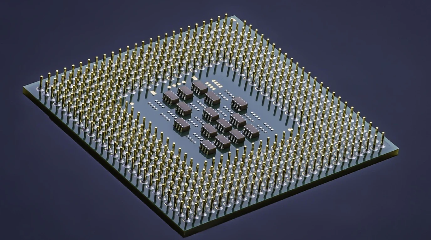
For the past three decades, high-performance general-purpose computing has been an unyielding duopoly: Intel/AMD x86 dominated high-power desktops and data center servers, while ARM proprietary licenses commanded mobile, automotive, and embedded edge systems. Open-source instruction set architectures (ISAs) like RISC-V were long dismissed by legacy silicon architects as academic toys suited only for simple microcontrollers and low-power IoT sensor motes. The SiFive Performance P550 core permanently shattered that narrative, proving that open-standard silicon can achieve modern out-of-order execution performance comparable to mainstream ARM application cores.
Direct Microarchitecture Verdict: SiFive Performance P550
The SiFive Performance P550 core is a 64-bit commercial RISC-V application processor implementing a 13-stage, triple-issue, out-of-order execution pipeline. Delivering a SPECint2006 score of 8.65/GHz, the P550 achieves performance parity with the ARM Cortex-A75 while occupying a significantly smaller physical silicon die area (0.24 mm2 on a 7nm process). It represents the definitive turning point where RISC-V transitioned from microcontroller status into high-throughput edge AI gateways, automotive domain controllers, and cloud micro-servers without proprietary ISA licensing royalty taxes.
The Pipeline Blueprint: 13-Stage Triple-Issue Out-of-Order Engine
To evaluate the engineering maturity of the P550, we must examine its microarchitectural pipeline. Early RISC-V cores (such as the SiFive U74 found in the StarFive VisionFive 2) were in-order processors: if an instruction stalled waiting for data to return from high-latency DDR memory, the entire processor core ground to a halt, wasting valuable execution cycles.
The P550 implements a full out-of-order (OoO) superscalar microarchitecture designed to maximize Instruction-Level Parallelism (ILP):
- Instruction Fetch & Advanced Branch Prediction: The front end fetches up to three instructions per clock cycle from a 32KB L1 instruction cache. It integrates a state-of-the-art TAGE (Tagged Geometric History Length) branch predictor paired with a Return Address Stack (RAS) and Branch Target Buffer (BTB). This speculative execution engine anticipates code jumps with over 95% accuracy, ensuring that the 13-stage pipeline remains saturated with useful instructions.
- Triple-Issue Decode & Rename: The decode stage decodes up to three 64-bit RISC-V (RV64GC) instructions per cycle, expanding compressed 16-bit instructions (RVC extension) on the fly without throughput penalties. Instructions pass through register renaming logic to eliminate false register dependencies (Write-After-Read and Write-After-Write hazards).
- Out-of-Order Scheduling & Execution Units: Renamed instructions enter a centralized reservation station and Reorder Buffer (ROB). Instructions are dynamically scheduled to fire as soon as their required operands become available—regardless of their original program order. The execution stage features multiple parallel execution pipes: two integer ALUs, a dedicated pipelined hardware integer divider/multiplier, and a fully IEEE 754-compliant floating-point unit (FPU).
- In-Order Retirement: Once executed, instructions are retired strictly in original program order through the Reorder Buffer, ensuring exact architectural state recovery and deterministic exception handling during page faults or external hardware interrupts.
| Microarchitectural Metric | SiFive Performance P550 | ARM Cortex-A75 (Reference) |
|---|---|---|
| Instruction Set Architecture | Open-standard RISC-V (RV64GCB) | Proprietary ARMv8.2-A |
| Pipeline Execution Model | 13-stage triple-issue Out-of-Order (OoO) | 11-to-13-stage 3-wide Out-of-Order (OoO) |
| SPECint2006 Benchmark Score | 8.65 / GHz | 8.60 / GHz |
| Silicon Die Area (7nm Process) | ~0.24 mm2 per core (excluding L2) | ~0.38 mm2 per core (excluding L2) |
| L1 Cache Configuration | 32KB Instruction + 32KB Data (ECC protected) | 64KB Instruction + 64KB Data |
| Multi-Core Cluster Scalability | Up to 4-core coherent cluster with shared L2/L3 | DynamIQ cluster up to 8 cores |
Vector Extensions: Integrating RVV 1.0 alongside Scalar Out-of-Order Execution
While the SiFive P550 core focuses on high-performance scalar integer and floating-point execution, modern data-parallel workloads require vector computing. In advanced silicon implementations (such as the SiFive Performance P650 and hybrid P550 multi-core platforms), the out-of-order scalar pipeline is tightly coupled with a dedicated RISC-V Vector (RVV 1.0) execution unit.
Unlike ARM’s fixed-width NEON vector engine (which is constrained to 128-bit vector registers) or x86 AVX-512 (which incurs heavy clock frequency downclocking penalties on server CPUs), the RISC-V Vector extension features Vector-Length Agnostic (VLA) architecture. Software compiled for RVV 1.0 dynamically configures its vector length (VLEN) at runtime. A compiled vector binary runs seamlessly on embedded silicon with 128-bit registers or on enterprise data center processors equipped with 512-bit or 1024-bit vector pipes without recompilation, providing unmatched cross-generational software longevity.
Linux Kernel Upstreaming and the Open Silicon Toolchain Ecosystem
The historical barrier to non-x86/ARM silicon adoption was software fragmentation. For years, alternative architectures required proprietary vendor-patched Linux kernels and custom GCC compilers that broke with every major operating system release.
The SiFive P550 stands out because its architectural definitions and extensions are 100% upstreamed into the mainline Linux kernel (Linux 6.4+), standard GNU Compiler Collection (GCC 13+), LLVM/Clang, and Debian/Ubuntu core package repositories. An enterprise engineer can boot a standard Debian or Ubuntu Server ISO directly on P550 silicon, compile native C/C++ or Rust applications with standard toolchains, and deploy standard Docker container microservices with zero proprietary vendor patches—achieving the exact same software simplicity long enjoyed by mainstream x86 and ARM platforms.
Silicon Density: The Real-Estate Efficiency of RISC-V
One of the most striking findings when auditing the P550’s physical layout is silicon area efficiency. Fabricated on a TSMC 7nm process node, a single P550 core occupies roughly 0.24 square millimeters of die area—nearly 35% smaller than an ARM Cortex-A75 delivering identical single-threaded performance.
This density advantage is a direct consequence of the RISC-V instruction set design. Unlike x86 (which carries forty years of legacy CISC instruction bloat requiring complex micro-op decoders) or ARM (which has accumulated significant legacy complexity across ARMv7, AArch32, and proprietary extensions), the RISC-V base integer ISA (RV64I) consists of fewer than 50 fundamental hardware instructions. Because instructions are fixed-width and regular, the P550’s instruction decoders require significantly fewer logic gates, drastically reducing static power leakage and freeing die area for larger cache hierarchies or integrated AI matrix accelerators.
Memory Subsystem and Multi-Core Coherency
A high-performance out-of-order core is only as good as the memory subsystem feeding it. The P550 implements a robust, enterprise-grade memory architecture:
- L1 Caches with SECDED ECC: Each core features 32KB of 4-way set-associative L1 instruction cache and 32KB of 8-way L1 data cache, fully protected by Single Error Correction, Double Error Detection (SECDED) error-correcting code for mission-critical reliability.
- Private L2 Cache Slice: Each core is paired with a private, low-latency 256KB to 512KB L2 cache slice operating at full core clock speed.
- Coherent Multi-Core TileLink Fabric: Up to four P550 cores are clustered together around a high-speed TileLink interconnect bus. TileLink maintains strict cache coherency across all cores and provides high-bandwidth access to a shared 4MB L3 cache and external DDR4/DDR5/LPDDR5 memory controllers.
Deterministic Real-Time Extensions: The CLIC and Physical Memory Protection
For mission-critical embedded control, the SiFive P550 integrates the Core-Local Interrupt Controller (CLIC) and Physical Memory Protection (PMP). Unlike legacy interrupt controllers that suffer variable latency, the CLIC provides prioritized, vectored interrupt handling with sub-15-cycle response times.
Furthermore, the P550’s PMP unit enforces hardware-level memory domain separation, preventing unprivileged software routines or compromised device drivers from accessing secure kernel memory regions, making the core ideal for safety-critical industrial automation.
The Strategic Significance: Sovereignty and Custom Silicon Freedom
The Open Silicon Industry Impact
The commercial success of the SiFive P550 represents a seismic shift for fabless semiconductor companies, aerospace systems integrators, and automotive OEMs:
- Freedom from Geopolitical Licensing Restrictions: Because the RISC-V international standard is managed by an open non-profit association based in Switzerland, enterprises can design custom application silicon without fear of unilateral export control blockades or aggressive IP license renegotiations from a single corporate vendor.
- Custom Instruction Extension Acceleration: Unlike proprietary ARM licenses (which strictly forbid modifying the instruction set), the RISC-V standard explicitly reserves opcode space for custom extensions. Silicon designers can embed proprietary hardware cryptographic accelerators, custom neural network instructions, or specialized DSP math pipelines directly into the P550 core execution pipeline.
To see how high-performance RISC-V cores are being paired with specialized edge AI NPUs, review our technical audit of Radxa Rock 5B+ vs Orange Pi 5 Max: RK3588 Benchmarks.
Explore our latest comprehensive breakdown on AMD XDNA 2 NPU Architecture: 50 TOPS Block Architecture.
Explore our latest comprehensive breakdown on Kneron KL720 NPU: Ultra-Low-Power Edge Vision Inference.
Explore our latest comprehensive breakdown on Hailo-8 M.2 vs Hailo-10: 40 TOPS Generative AI on Edge.
Explore our latest comprehensive breakdown on Milk-V Pioneer RISC-V Workstation: 64-Core SG2042 TCO.
Explore our latest comprehensive breakdown on Qualcomm Snapdragon X Elite NPU: 45 TOPS On-Device LLMs.