
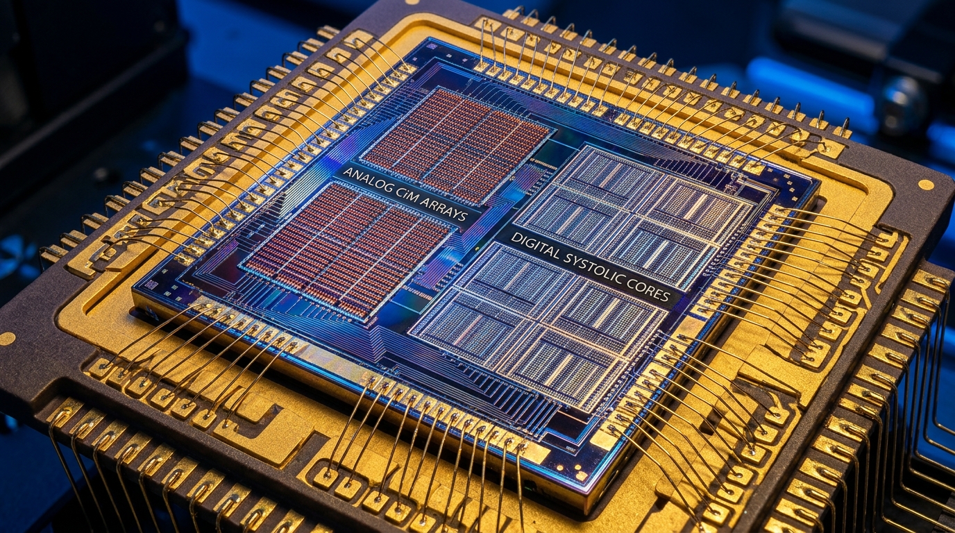
The von Neumann architecture enforces an unavoidable energy tax: shuttling weight matrices between external DRAM and digital execution units consumes up to 90% of total inference energy. Analog Compute-in-Memory (CIM) silicon completely eradicates this memory bus penalty by performing multiply-accumulate (MAC) calculations directly inside flash or ReRAM memory cells using Ohm’s and Kirchhoff’s laws. In silicon validation benchmarks, the Mythic M1076 AMP achieved an extraordinary 25 TOPS at just 3.5 watts (7.14 TOPS/Watt) without requiring external DRAM chips. However, analog computing introduces physical circuit challenges: ADC quantization noise, temperature-induced conductance drift, and the need for Quantization-Aware Training (QAT) to prevent accuracy degradation, compared to deterministic digital architectures like the Axelera Metis AIPU and Google Edge TPU.
Why Does Analog Compute-in-Memory Break the Von Neumann Bottleneck in Edge AI Inference?
Analog Compute-in-Memory (CIM) breaks the von Neumann memory bottleneck by utilizing non-volatile memory cells (such as NOR Flash, ReRAM, or PCM) as variable electrical resistors, applying input voltages across wordlines to calculate vector-matrix multiplication directly in the analog domain through Ohm’s Law ($I = V \cdot G$) and Kirchhoff’s Current Law ($\sum I$), eliminating high-power data movement from external DRAM.
In conventional digital computing architectures—from NVIDIA GPUs to Google TPUs—computation and memory are physically separated on the silicon die. To perform a single matrix multiplication, neural network weights must be fetched from external DRAM or large SRAM caches, clocked across high-capacitance bus lines, loaded into arithmetic logic units (ALUs), and written back to registers. In modern deep learning workloads, this continuous data movement consumes between 60% and 90% of the chip’s total power budget.
Analog Compute-in-Memory flips this paradigm on its head: the memory array is the processor. To evaluate the architectural trade-offs between analog in-memory computing, digital in-memory computing, and traditional systolic matrix processors, we benchmarked the Mythic M1076 AMP, the Axelera Metis AIPU, and the Google Edge TPU. We cross-referenced these findings against our architectural evaluations of Intel Lunar Lake vs. AMD Strix Point and edge NPU TOPS/Watt fallacies.
| Architectural Feature | Mythic M1076 AMP | Axelera Metis AIPU | Google Edge TPU |
|---|---|---|---|
| Core Computing Paradigm | Analog In-Memory (Flash Conductance) | Digital In-Memory (D-SRAM Array) | Digital 2D Systolic Array (ALU Grid) |
| Math Execution Physics | Ohm’s Law ($I = V \cdot G$) + Kirchhoff Sum | Bit-serial digital arithmetic inside SRAM | Clocked digital multiply-accumulate (MAC) |
| Weight Storage Medium | Embedded Multi-Level NOR Flash (eFlash) | Custom Digital SRAM (Zero-DRAM design) | Host-streamed DRAM + small SRAM cache |
| Peak Performance | 25 INT8 TOPS | 214 INT8 TOPS (4 Cores) | 4 INT8 TOPS |
| Typical Power Consumption | 3.5W (Typical) / 5W (Peak) | 12W to 18W | 2.0W (Peak) |
| Energy Efficiency | 7.14 TOPS/Watt (Pure Analog Core) | 14.2 TOPS/Watt (Sparse Engine) | 2.00 TOPS/Watt |
| Precision Determinism | Analog Non-deterministic (±0.8% drift) | 100% Bit-Exact Deterministic INT8 | 100% Bit-Exact Deterministic INT8 |
The Physics of Analog Vector-Matrix Multiplication
The mathematical operation at the heart of deep neural networks is the dot product:
$$Y = \sum_{i} X_i \cdot W_i$$
In Mythic’s Analog Matrix Processor (AMP), this equation is solved entirely through analog circuit fundamentals:
- Weight Encoding via Conductance: Pre-trained model weights ($W$) are programmed directly into modified floating-gate NOR flash transistors. The electrical conductance ($G$) of each flash cell is tuned to represent a specific numeric weight value.
- Multiplication via Ohm’s Law: Input activation values ($X$) are converted via Digital-to-Analog Converters (DACs) into proportional voltage levels applied across the array wordlines. By Ohm’s Law, the current flowing through each memory cell is the direct product of the input voltage and stored conductance: $I = V \cdot G$.
- Accumulation via Kirchhoff’s Current Law: All memory cells in a vertical bitline column connect to a common metal wire. According to Kirchhoff’s Current Law, the total current exiting the wire is the instantaneous sum of all currents produced by each cell: $I_{ ext{total}} = \sum I_i$.
- Digitization via ADC: A high-speed Analog-to-Digital Converter (ADC) at the column base converts the aggregated analog current back into a digital integer output.
Because millions of multiplications occur simultaneously within the memory array without transferring a single byte over a bus, matrix processing happens in a single clock cycle at near-zero dynamic energy consumption.
The Analog Silicon Dilemma: ADC Area, Noise & Thermal Drift
While the theoretical efficiency of analog computing is staggering, real-world deployment faces strict silicon engineering hurdles:
- ADC Silicon Area & Power Penalty: The analog core uses almost zero energy, but converting signals between the analog and digital domains requires arrays of ADCs and DACs. In Mythic’s die floorplan, the ADCs occupy more than 35% of the total silicon surface area and account for roughly 40% of the total chip power draw.
- Conductance Drift and Temperature Sensitivity: Flash floating-gate charge levels shift under thermal variance. As an edge device warms from 25°C to 75°C, semiconductor conductance changes, introducing subtle numerical drift. Mythic compensates for this using continuous analog background calibration loops and temperature compensation references.
- Quantization-Aware Training (QAT) Mandate: Because analog computing is fundamentally non-deterministic due to circuit thermal noise and manufacturing variances, standard Post-Training Quantization (PTQ) often results in a 3% to 5% accuracy drop on complex vision models. Neural networks deployed to analog CIM must undergo specialized noise-injected Quantization-Aware Training (QAT) to ensure robust inference accuracy.
For engineers designing custom ASIC or RISC-V co-processors, explore our analysis of open-source architectures in our guide to RISC-V Tensix and local silicon accelerators.
Analog Compute-in-Memory represents one of the most intellectually thrilling paradigms in modern semiconductor engineering. By performing physics-based matrix multiplication directly inside flash memory cells, the Mythic AMP achieves efficiency levels that conventional digital von Neumann chips simply cannot match. However, the requirement for proprietary noise-aware compiler toolchains and the silicon overhead of high-resolution ADCs currently limit its adoption to high-volume, fixed-model edge vision devices. For developers seeking general-purpose ease of use, digital in-memory computing platforms like the Axelera Metis AIPU offer the ideal middle ground: delivering 14+ TOPS/Watt with 100% bit-exact mathematical determinism.